ACA, U of A launch $35.5M semiconductor tech center
The Arizona Commerce Authority’s funding of tools and augmented reality training systems for advanced semiconductor manufacturing boosts workforce development and research partnerships.

FAB TOUR: A ribbon-cutting ceremony on Feb. 17 at the Electrical and Computer Engineering Building celebrates a three-year endeavor to extend capabilities of computer chip center at the University of Arizona.
As the state anticipates adding over 25,000 new jobs in the semiconductor industry, the Arizona Commerce Authority and the University of Arizona are strengthening the workforce pipeline with a $35.5 million facility expansion.
University, government and industry leaders unveiled the Office of Research and Partnerships’ Nano Fabrication Center semiconductor cleanroom with a ribbon-cutting ceremony on Feb. 17.

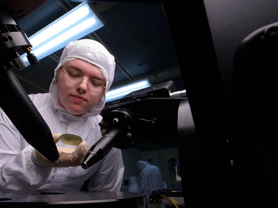
Gregory Book (far right), director of the University of Arizona’s Nano Fabrication Center, explains that the cleanroom's lights have a yellowish hue to protect UV-sensitive materials.
“Semiconductors power nearly every part of modern life, from health care and transportation to clean energy, national security and artificial intelligence,” said Gov. Katie Hobbs. “For too long, much of this manufacturing capacity existed overseas. Arizona has stepped forward to change that.”
Located in the Electrical and Computer Engineering Building, the cleanroom prepares students for the state’s booming tech sector while supporting faculty research and industry collaboration on chip fabrication, optical devices and quantum computing systems.
“The University of Arizona’s cleanroom expansion opening marks a significant milestone in advancing semiconductor innovation in Arizona," said Sandra Watson, president and CEO of the Arizona Commerce Authority. “We’re proud to collaborate with the University of Arizona and all of the partners involved to support this state-of-the-art facility – advancing semiconductor R&D and reinforcing Arizona’s position as an epicenter for pioneering semiconductor innovation and investment.”
The Arizona Commerce Authority awarded funding in 2023 to expand the cleanroom from 2,800 to 6,800 square feet, equip it with ultramodern tools, and support a statewide workforce development program.

'We have collaborated with multiple companies to support their research and development efforts and look forward to growing our network of partners to promote Arizona's semiconductor manufacturing industry,' says Krishna Muralidharan, director of the Center for Semiconductor Manufacturing and professor of materials science and engineering.
“My sincere thanks to Gov. Katie Hobbs and the Arizona Commerce Authority for their partnership in advancing this investment,” said U of A President Suresh Garimella. “By aligning world-class capabilities with hands-on learning for our students, we are strengthening Arizona's competitiveness and fulfilling our land-grant mission to create opportunity across our state.”
Cleanroom fast-tracks progress
Expansion brought a metrology bay and overhauled infrastructure.
The facility’s air is 10,000 times cleaner than outside air – essential for exacting protocols that ensure the purity, precision and reliability of chips.
Among equipment is an ultrasensitive infrared emissions microscope, donated by optics company IRLabs, which detects chip failures before they happen.
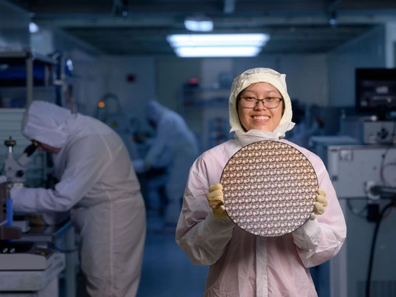
A dedicated bay houses chemical and mechanical polishing equipment to smooth silicon wafers – the foundation of semiconductor chips. U of A’s planarization bay is among the first university cleanrooms to support 12-inch wafer polishing.
Additionally, the facility handles photolithography, etching, metrology and packaging – critical steps in producing nanoscale technology.
“This clean room is where ideas move from concept to capability for the global semiconductor industry,” said Tomás Díaz de la Rubia, senior vice president for research and partnerships. “By integrating advanced fabrication and photonics with talent development, the Center for Semiconductor Manufacturing has created an environment where faculty, students and industry partners can build and test the semiconductor technologies of the future.”

Mechanical engineering junior Ben Nguyen (left) presents an augmented reality headset training at the Feb. 17 event. Electrical and computer engineering assistant professors Soheil Salehi and Pratik Satam, along with students John Martin Encinas, Veeramani Pugazhenthi, Josh Dean and Sujan Ghimire were instrumental in setting up the AR classroom.
Next door, undergraduates tap into streamlined training with Apple Vision Pro and Meta Quest 3 headsets, where up to 18 students explore digital twins of the cleanroom and its equipment.
The classroom supports the university’s undergraduate degrees in microelectronics packaging and semiconductor manufacturing, as well as stackable graduate degree certificates.
Bridge from classroom to jobs
The Arizona Commerce Authority allocated $4.5 million of its original $35.5 million investment for workforce development that extends beyond campus, positioning U of A as a bridge between education and high-paying careers.
"The benefits of Arizona Commerce Authority's investment will extend far beyond the University of Arizona campus, supporting Arizona’s role as the national leader in micro- and nanofabrication," said David W. Hahn, the Craig M. Berge Dean of the College of Engineering. "This project speaks to the power of collaboration between the ACA and our university, accelerating Arizona’s workforce development, and driving technological advancement in fulfillment of our commitment to shaping the future through research and innovation."
The Southwest Nano-Lab Alliance – a coalition of the state’s three public universities, the University of Utah, the University of New Mexico and Rio Salado College – collaborates on workforce initiatives. Augmented reality teaching modules will be shared with regional partners like Pima Community College and Central Arizona College via the SemiXperience platform. Additionally, semiconductor manufacturing courses, along with corresponding teaching resources, are available on the SemiSphere content-sharing platform.

Augmented reality teaching modules fast-track basic training in semiconductor manufacturing for undergraduates.
K-12 programs are already bolstering the pipeline. The Chips and Wafers Camp, a high school summer camp developed with Chandler Unified School District, introduces high schoolers to the industry.
“Arizona’s semiconductor future depends on skilled technicians, engineers and innovators ready to step into high-tech jobs,” Hobbs said. “Through hands-on training, advanced simulation tools and partnerships across the state, the University of Arizona is creating pathways into these careers.”
Additional cleanroom industry partners include Araca, Arizona Optical Metrology, BASF, Cactus Materials, Edgehog Advanced Technologies, GmbH, Intel, Leonardo, Micro-Hybrid Electronics, Norcon Technologies, TSMC and Wolf Biotechnology.